Home Products

Compound semiconductor wafer inspection

Compound Semiconductor Inspection Service (CSIS)

Analytical Testing Service

MONSTR Sense Technologies’ Compound Semiconductor Inspection Service (CSIS) enables external organizations to access our proprietary, multi-modal ultrafast imaging microscope technology, facilitating informed tool purchasing decisions. CSIS provides sensitive and specific detection and classification of defects in wide-bandgap semiconductors, including those within substrate wafers and epitaxial layers, as an Analytical Testing Service. Our Ultrafast Imaging technique is relatively background-free, producing high-contrast detections of killer defects in several modalities: whole wafers (overview scans), high resolution, and volumetric images. CSIS defect inspection reports are designed to support wafer growth recipe research and development, as well as failure analysis evaluations.

We currently offer three service packages:

CSIS Preferred:
  • Linear absorption (LA) defect inspection analysis across an entire wafer (up to 8″) with survey scan resolution (4 um)
  • Transient absorption (TA) defect inspection analysis across an entire wafer (up to 8″) with survey scan resolution (4 um)
  • High-resolution (<1 um) scans of representative defect areas
  • Defect Inspection Report with location and classification of Defect Classes (KLARF File)
CSIS Premium:
  • Linear absorption (LA) defect inspection analysis across an entire wafer (up to 8″) with survey scan resolution (4 um)
  • Transient absorption (TA) defect inspection analysis across an entire wafer (up to 8″) with survey scan resolution (4 um)
  • High-resolution (<1 um) scan of representative defect areas
  • Volumetric scan of representative defect areas

Defect Inspection Report with location and classification of Defect Classes (KLARF File)

CSIS Custom:
  • Engage with our Ultrafast Imaging & Defect Inspection Experts to develop a Customized Defect Inspection Project that addresses your unique needs. Customized Projects are typically based on first conducting a Pilot Study to establish the optimal set of defect inspection conditions for your samples.
Materials SiC, GaN, GaAs
Wafer size 2″, 4″, 6″, 8″
Spatial resolution (lateral) 1-4 microns
Spatial resolution (axial) down to 3 microns
Measured channels Linearabsorption (LA), Transient absorption (TA)
Wavelength range (for selectivity) 350 nm-650 nm, 690 nm-1000 nm

Here’s why we think you should try our nonlinear imaging to inspect your SiC and GaN wafers:

  1. Nonlinear imaging reveals more than morphology: we measure defects that impact electronic structure.  There are many things lighting up in a scattering image: Killer defects as much as non-killer defects, particulates, and dust. Our technique is resonant – if the defect does not alter the bandstructure, we can tell.
  2. Surface, subsurface, and substrate defects. Scattering is only sensitive to surface defects. A photoluminescence excitation beam can only penetrate so deep into the material. Our excitation beam penetrates deep and is sensitive to surface, subsurface, and even substrate defects. 
  3. Nonlinear imaging is coherent, and therefore it is fast. Our nonlinear imaging is a coherent technique. This means we can go to larger spots without compromising signal collection. It also means we can go to sub-microsecond pixel dwell times, which enables high throughput (<10 mins) whole wafer scanning.

Nonlinear optical measurements solve some problems of white-light imaging and photoluminescence. Nonlinear measurements, particularly four-wave mixing, are sensitive to fundamental defects in the crystalline structure of the semiconductor that impact the carriers. Therefore, defects, even subsurface defects, will be visible in the four-wave-mixing image if the defect has a appreciable impact on the electrical properties of the semiconductor.

Compound semiconductors are the backbone of high-power electronics, high-frequency electronics, and opto-electronics. As global demand for compound semiconductors grows, improving yield rates of materials such as gallium nitride (GaN) and silicon carbide (SiC) is more important than ever. By developing better optical inspection tools, we help manufacturers identify yield-killing defects in substrates and epitaxy layers long before the material is used in device production.

MONSTR Sense Technologies’ products are being used in research labs worldwide to improve the development of SiC and GaN devices, two-dimensional materials such as graphene and transition metal dichalcogenides, perovskites, colloidal quantum dots, gallium arsenide (GaAs)-based devices, and quantum materials such as vacancy centers.

Our ultrafast nonlinear imaging inspection technique is highly versatile – we work with tunable excitation lasers that allow us to study materials with bandgaps over the broad ranges 1.9-3.5 eV (wavelengths 350-650 nm) and 1.25-1.75 eV (690-1000 nm). This makes the technique perfectly suitable for most compound semiconductor materials of interest, including SiC, GaN, and GaAs.

Silicon Carbide

SiC 6″ wafer image, select defects marked

Silicon Carbide (SiC) is the current focus for many high-power electronics manufacturers. The purpose of inspection tools is to distinguish between killer and non-killer defects. Because our nonlinear imaging technique is highly sensitive to small changes in the bandstructure, killer defects that affect device performance show up via an increase or decrease in the transient absorption (TA) signal.

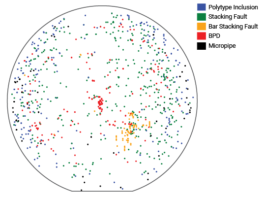
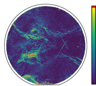
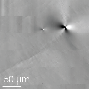
As part of the CSIS defect analysis, we typically image 6″-8” SiC wafers with a 4 um spot size and classify defects across the entire wafer in a survey scan. Upon request, we also collect high-resolution scans with sub-micron resolution in specific areas. Examples of high-resolution scans of some defects of interest in SiC are shown below, including examples of high-resolution volumetric scans.

Surface triangles glow in a nonlinear image through the entire volume of the triangle. Stacking faults glow more weakly and have a thickness that is less than our axial resolution. The brightness of the TA response can be used for stacking fault classification, with stacking faults that have more detrimental effects on the bandstructure having a stronger TA response.

Our tools are not only sensitive to epilayer defects. Even substrate defects, such as basal plane dislocations, threading dislocations, and micropipes, show up in the nonlinear image. Unlike photoluminescence (PL), our technique does not rely on above-gap excitation, therefore, we are more sensitive to deep defects in the epilayer and substrate if the focus is set accordingly.

The signal from our ultrafast imaging modality is emitted from the microscope focus, which provides <5 um axial resolution in the SiC with our 0.85 NA objective. Since we also excite with light that transmits through the entire wafer, MONSTR Sense’s ultrafast imaging can measure deep within the wafer. Below, we show volumetric images of SiC surface triangle defects in the epitaxy layer, in which we measure the volume of 3C of polytype inclusion. We offer volumetric scans through entire wafers with high axial resolution.

Gallium Nitride

Surface heterogeneities (triangular pyramids) are readily visible in the Mg-doped, P-type GaN Templates grown on (0001) sapphire substrates by low-pressure metal organic chemical vapor phase deposition (MOCVD). Surface heterogeneity is likely due to stacking fault formation and three-dimensional growth). It is reported that the density and size of these structures increase with the amount of magnesium incorporated into the GaN samples.

Compared to SiC, bulk GaN has a long decay time, evidenced in the figure below by a signal lasting well past 50 ps. Defects remain distinguishable by signal enhancement and changes in the decay time. Because GaN is a direct gap semiconductor, the bandstructure can interact well with light without the introduction of phonons. Beyond defect characterization, four-wave mixing has proven powerful for the measurement of excitons in direct gap semiconductors. The direct gap in the bandstructure allows for excitons, and it is part of the reason GaN measurements with nonlinear imaging and photoluminescence are so different from SiC.

Gallium Arsenide

 Gallium Arsenide (GaAs) has made it from the lab to the marketplace with applications including integrated circuits, LEDs, and solar cells. Defect inspection of GaAs and GaAs quantum wells remains at the forefront of the industry. However, correlating defects with their impact on device performance and measuring subsurface defects is challenging.

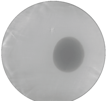
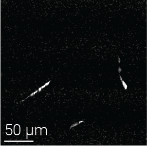
Full wafer scans of a multiple quantum well sample highlight some features unique to these samples. For one, thickness variations in the substrate lead to Fabry-Perot fringes in the wafer image. Secondly, many of the defects in the wafer manifest themselves through bright emission properties. The provided wafer excerpt has a diameter of 2″, though wafers of up to 6″ can be scanned with sub-10 um resolution. Moreover, we offer the option to provide high-resolution images of certain defect areas, as illustrated below.

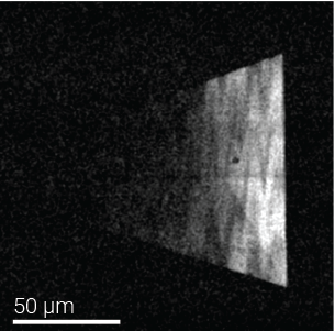
Scratches, as well as crystallographic defects, show up strongly in the FWM. Additionally, defects that partially or fully emit brightly can also be found with our nonlinear inspection method. Those defects are crucial because conventional brightfield or darkfield microscopy is often not sensitive to them. However, they clearly alter the bandstructure of the material, affecting the electrical properties and hence often acting as a killer defect. Our nonlinear imaging is also sensitive to subsurface defects that do not show up in any surface-sensitive scattering technique.

For more information or to get a quote, reach out to us at info@monstrsense.com or send us a message on our contact page.