

Hypertemporal Imaging & Defect Contrast
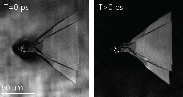
Figure 1. Defect visibility for T = 0 ps (pump & probe pulse are overlapped) vs. T> 0 ps (pump & probe pulse are not overlapped)
With ultrafast temporal resolution, the KRAKEN BLUE microscope is able to measure ultrafast decay processes. Using ultrafast imaging users can also enhance contrast in an image using the ultrafast decay time.
Defect Contrast Application: defects in many compound semiconductors, such as silicon carbide or gallium nitride, will trap electrons. Hypertemporal imaging distinguishes material regions based on the decay time of an excitation in the material. An example defect, a polytype inclusion in silicon carbide, is shown above. When the pump and probe pulses are overlapped (T = 0 ps), the signal is dominated by the bulk contribution. When there is a finite delay between the two pulses (T > 0 ps), the bulk signal has decayed, while the long-lived trapped states isolated to defect sites lead to a glowing defect feature. The hypertemporal contrast mechanism offers KRAKEN BLUE users the ability to measure background-free signatures of defects.
Volumetric Imaging
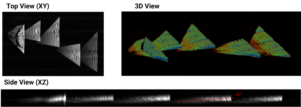
Figure 2. 3D Morphology of a stacking fault cluster in silicon carbide.
Ultrafast imaging is a nonlinear imaging technique that relies on the nonlinear interactions of pump and probe pulses in the material of interest. Signals resulting from nonlinear optical processes are primarily emitted at the laser focus, where the light is most intense. Ultrafast imaging is therefore capable of isolating narrow slices within the material and enabling volumetric imaging with an axial resolution comparable to that of two-photon microscopy.
An example of volumetric images for a stacking fault cluster in SiC is shown above. Volumetric imaging measured using the KRAKEN BLUE microscope enable manufacturers to determine the 3D morphology, depth, and origin of defects.
Hyperspectral Imaging
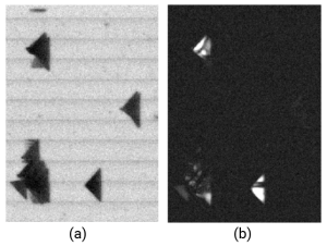
Figure 3. (a) Photoluminescence image at the bulk band of silicon carbide, highlighting defects in epilayer. (b) Photoluminescence image in the visible range, highlighting defects in epilayer.
Hyperspectral Imaging enables users of the KRAKEN BLUE microscope to tune the wavelengths of the tool to the material or defect of interest. An example of hyperspectral imaging, utilizing our optional photoluminescence add-on, shows distinct spectral responses of various epilayer defects.
Detection & Classification of Defects in Wide Bandgap Semiconductors
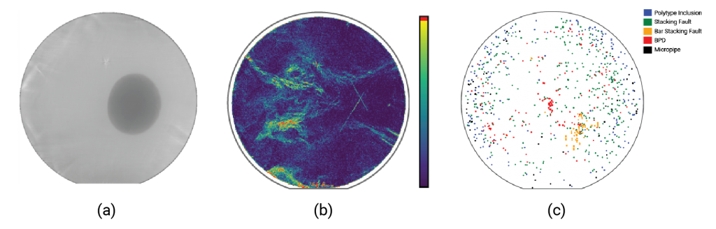
Figure 4. From raw data to defect detection in SiC: (a) Raw wafer image (b) Threading dislocation defects in the substrate, measured through the epilayer (c) Epi-layer defect map of select defects
The KRAKEN BLUE microscope can be used to detect silicon carbide defects at high throughput, up to 8 min/6″ wafer. Our multi-channel measurements enable the detection of both substrate and epilayer killer defects, including basal plane dislocations, threading dislocations, micropipes, and stacking faults with classification, in wafers up to 8″. KRAKEN BLUE can also be used for other wide bandgap compound semiconductors, such as gallium nitride.
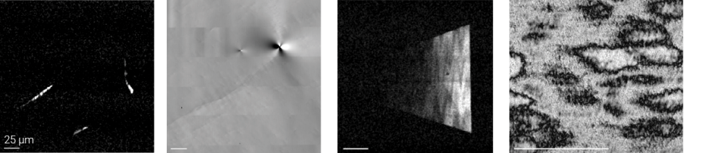
Figure 5. Key defects in wide-bandgap compound semiconductors: (a) Basal plane dislocations in SiC substrate (b) threading dislcoations & micropipes in SiC substrate (c) stacking fault in SiC epilayer (d) Grain boundaries in GaN template.
Related Publications
- Joint white paper with Light Conversion featuring ultrafast microscopy for material characterization
- Joint white paper with Coherent featuring the applications of ultrafast microscopy to 2D materials
- Rapid ultrafast microscopy for characterizing chemical-vapor deposition (CVD)-grown materials
- High-Speed Spectroscopic Transient Absorption Imaging of Defects in Graphene
- [FEATURED] Imaging dynamics in transition metal dichalcogenide heterostructures
- Pump-probe imaging microscopy to characterize historic artwork
- Pump-probe imaging microscopy to differentiate melanoma tissues
UV-Tunable Wavelength
KRAKEN BLUE has automatic wavelength tuning, automatic focus control, and automatic alignment control. This enables rapid adjustment of wavelengths with the click of a button and without any user-alignment changes.
Minimal User Training
Inspection of compound semiconductor defects with the KRAKEN BLUE microscope is fast and accessible:
- Easy-to-use imaging interface
- Eye safe
- Non-contact, non-destructive
Stable Alignment
Collinear optical design made to maintain long-term alignment, which is unprecedented for ultrafast spectroscopy and imaging systems.
Active controls are engineered to manage beam pointing change through wavelength tuning from 350-500 nm, along with normal beam-pointing fluctuations of the included ultrafast laser.
KRAKEN BLUE Ultrafast Microscope Specifications
| Specification | Standard System | |
|---|---|---|
| Tunable wavelength range | 350-500 nm | |
| Illumination power (at sample) | 3-25 mW | |
| Decay time range | 0-2000 ps | |
| Bandwidth-limited pulse duration | <140 fs | |
| Compatible sample mounting | X-Y stage, Cryostat | |
| Lateral Resolution | < 1 um | |
| Axial resolution | <8 um (< 3 um) | |
| Detection Image Frame Rate | 1 fps (20 fps upgrade) | |
| Dimensions | 62 in x 35 in x 65 in |
SiC-specific Specifications
| Specification | Standard System | |
|---|---|---|
| Wafer Holder | 6″/150 mm & 8″/200 mm | |
| Spatial Resolution | 500 nm – 8 um | |
| Wafer Throughput | Up to 7 wafers (6″)/hour | |
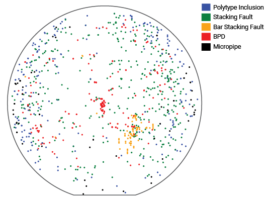
| Select Defect Sensitivity | Polytype Inclusion, Stacking Faults, Micropipes, Threading Dislocations, Basal Plane Dislocations |
Try it out with a service inspection
Try out KRAKEN BLUE and ultrafast microscopy with our Compound Semiconductor Inspection (CSIS) Service.
Compound Semiconductor Inspection Service
We offer a characterization service for the characterization and inspection of your compound semiconductor wafers,
This is a great way to test how MONSTR Sense products can fit into your materials growth process and explore the advantages of ultrafast imaging.
For more information or to get on our mailing list, please reach out to us at info@monstrsense.com or use our contact page.