Silicon Carbide (SiC) Processing for Devices
SiC-based power electronics offer several advantages over conventional Si devices, which include: (1) operation at higher electric fields and higher temperatures with better reliability than Si-based power electronics due to a wide bandgap (3.3 eV for 4H-SiC); (2) improved thermal conductivity (3X that of Si), which enables higher power density packaging for SiC devices with better heat dissipation; and (3) superior saturation electron velocity (2X that of Si) allows for higher frequencies of operation with lower switching losses than Si-based power devices. The physical properties of SiC make it preferred for the development of electronic devices, including power MOSFETs with high blocking voltage and low on-resistance and Schottky barrier diodes (SBD) that can withstand large breakdown fields with small reverse leakage currents.
Silicon carbide is grown as a boule: a large, nominally single-crystal cylinder. The boule is sliced into thin substrate wafers, which are polished. Epitaxial layers are grown on the substrate. The typical polytype that is grown for power electronic applications is 4H-SiC. The substrates are typically sliced 4º off of the c-axis. During epitaxy growth, an initial buffer layer is used to reduce defect propagation from the substrate, and the full epitaxy is then grown to be a few microns thick.
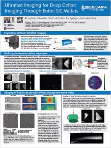
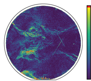
Defect inspection is used at every step of the wafer production process to qualify the processing steps, feed forward defect information for die mapping, and feed back killer defect densities for yield improvement.
Epilayer Defects
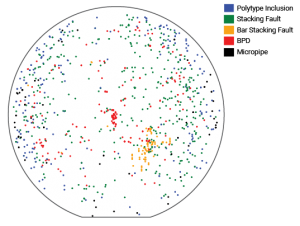
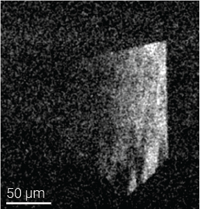
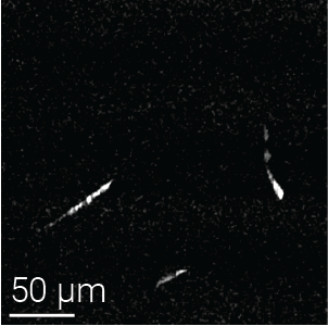
Defects in the epilayer of SiC are most directly correlated with device failures. These defects are typically seeded by a crystallographic defect or particle downfall at the substrate surface. For instance basal plane dislocations (BPDs) in the substrate have the potential to convert into killer defects in the epitaxy such as stacking faults (SFs) or epitaxy BPDs.
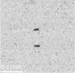
Conventional methods for detecting epitaxy defects include surface scatter imaging and photoluminescence (PL) imaging. Many killer defects such as BPDs and SFs, are not visible in surface channels. High-throughput PL imaging, which measures bulk PL, can see subsurface defects, but it cannot distinguish between types of SFs and polytype inclusions.
In the figures below we show how Ultrafast Imaging is not only able to detect all killer epilayer defects, but the Transient Absorption (TA) channel is also able to classify triangular defects. Based on signal intensity TA can distinguish polytype inclusions, more-killer SFs (such as Shockley SFs), and less-killer SFs (such as intrinsic Frank SFs). Because TA is sensitive to how defects impact band structure, the brightest defects are the most likely to be killer! We are able to record 3D volumetric images of those features to see defect origins, morphology, and to visualize defect clusters.


What makes Ultrafast Imaging so powerful?
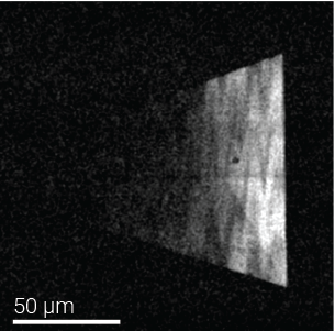
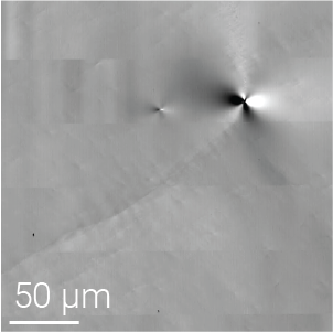
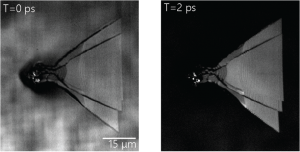 Ultrafast lasers create an excitation in semiconductors at a timescale that is nearly instantaneous compared to all physical relaxation processes within the material. The excitation is deterministic, and the time scale of relaxation processes becomes a source of defect contrast. For instance, an excitation of bulk SiC relaxes almost instaneously, while defect areas containing trapped states will have decay times on a much longer timescale. In the adjacent figure we show that using a TA measurement tuned to a finite decay time, ultrafast imaging offers a background-free measure of select defects in SiC.
For More Information check out the MONSTR Sense poster from the International Conference on Silicon Carbide and Related Materials (ICSCRM) 2025: